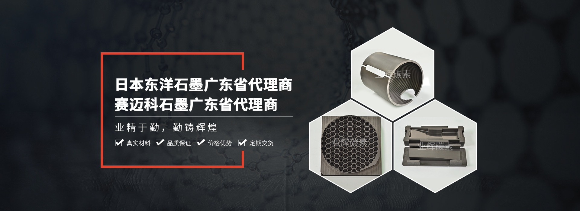
Electronic information semiconductor graphite
时间:2022-07-28 浏览次数:2192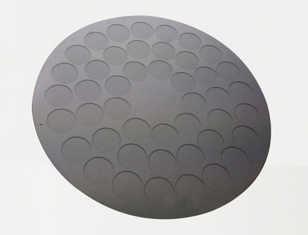
Graphite deposited silicon carbide base is a component used to support wafers in the process of depositing semiconductor thin film materials on the surface of wafers. It is mainly used in metal organic chemical vapor deposition (MOCVD) equipment. The base material of the product is high-purity graphite, and there is a layer on the surface with a thickness of about 110 μ m±15 μ M U.M thick dense silicon carbide film, which is obtained by chemical vapor phase deposition (CVD) process. Its function is to avoid the pollution of the wafer caused by the outgassing of the graphite matrix under high temperature conditions, and improve the thermal shock resistance, oxidation resistance, mechanical strength and chemical gas corrosion resistance of the graphite matrix. In this study, a kind of high density and high purity graphite is used as the matrix, and its thermal expansion coefficient is close to silicon carbide; Using methyl trichlorosilane (ch3si CL3, abbreviated as MTS) as the gas source and H2 as the carrier gas, a high-purity, dense, uniform and defect free silicon carbide film was formed on the surface of graphite substrate under certain process parameters such as furnace pressure and temperature. The microstructure, chemical composition and film quality of the film were observed, analyzed and evaluated.
It is applied to semiconductor, integrated circuit, flat film display, LED chip, photovoltaic solar energy, optical optical communication, optical magnetic storage, electronic packaging, electric new energy, Low-E glass, decorative coating, tool coating and other fields.